Ultraviolet Germicidal Bulb,Portable Uv Lamp,Uv Light Bulbs For Humans,Nb Uvb Lamp Guangdong Kingrate Optoelectronic Technology Co., Ltd. , https://www.kingrateuv.com
How to form large-area high-quality graphene on an insulating substrate is still a problem. Therefore, whether it is to explore a new method for preparing graphene, or to find a suitable base material for growing graphene, in order to present the novel physical properties of graphene at room temperature, it is an urgent need to solve the basic research and device application of graphene. The problem.
Diamond is an insulating material with many excellent properties. If graphene can be fabricated on a diamond substrate, it is advantageous to exhibit graphene special mechanical, thermal, electrical and optical properties at room temperature compared to other substrate materials. Performance is an ideal structure for constructing graphene novelty devices. But so far, studies on the direct preparation of graphene on the diamond surface have rarely been reported.
Recently, Prof. Gu Changzhi, Researcher of the Institute of Physics of the Chinese Academy of Sciences/Beijing National Laboratory for Condensed Matter Physics, and Li Wujie, Li Junjie, and the researcher of Xu Quanfang, Quantum Science Simulation Center, Associate Professor Xu Jing of Renmin University of China and Rensselaer Polytechnic of the United States Professor Zhang Shengbai's cooperation, starting with material design, theoretically predicted that the diamond (111) surface can realize the phase transition of the diamond structure to the graphene structure under the induction of B atoms. After that, the experiment verified the single crystal diamond ( 111) The surface can be self-organized to form high quality graphene under B-doping conditions, and the number of layers is controllable. 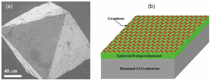
After that, they achieved the self-organized growth of graphene by CVD method on the (111) surface of high temperature and high pressure (HPHT) diamond single crystal by boron doping and growth parameter control. The prepared graphene has high quality. Low defect, large area and high mobility. Furthermore, it is possible to prepare graphene from a single layer to a double layer and a plurality of layers on a diamond substrate by changing the growth conditions, which is a good proof of the theoretical prediction. The graphene material on the diamond substrate, taking into account the many excellent physical properties of diamond and graphene, laid the foundation for the development of novel functional graphene devices. 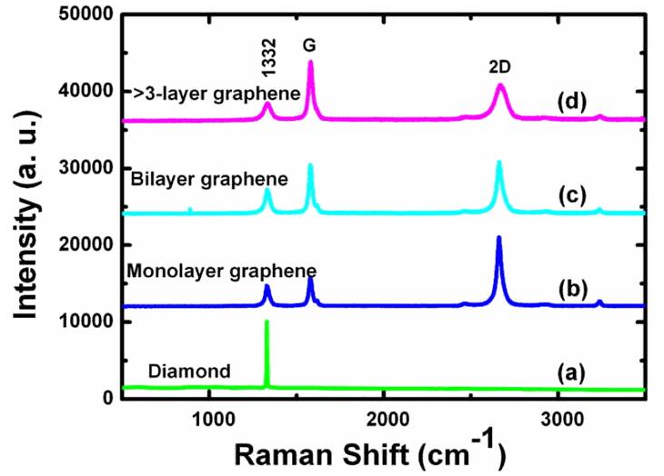

The above work has been funded by the National Natural Science Foundation of China, the Ministry of Science and Technology and the Chinese Academy of Sciences.
Article link: http://scitation.aip.org/content/aip/journal/apl/109/16/10.1063/1.4964710
Team leader introduction
Gu Changzhi: Male, received a Ph.D. in condensed matter physics from Jilin University in 1997. From 1991 to 2001, he worked as a professor at the State Key Laboratory of Superhard Materials at Jilin University. In 1997-1999, 2001 and 2004, he was engaged in cooperative research at the Fraunhofer Institute in Germany, the Physics Department of the Free University of Berlin, Germany, and the National Institute of Materials Research (NIMS). Now working in the micro-processing laboratory of the Institute of Physics of the Chinese Academy of Sciences, he is a researcher and doctoral tutor.
Main research directions: controllable preparation of nanomaterials and nanodevices, research on novel physical properties and application in information technology. Past major work and achievements: carbon represented by diamond, carbon nanotubes and graphene Controllable preparation of basic nanomaterials; found novel physical properties of carbon-based nanomaterials with size change at room temperature, such as multi-channel ballistic transport properties of electrons in multi-walled carbon nanotubes, laying a foundation for application in electronic devices Based on the movement of magnetic domain walls in metal nanostructures, a new type of low-power magnetic logic circuit is constructed. He has published more than 200 papers in internationally renowned academic journals such as Nature, PRL, Nano Letters, and JACS. Others have cited more than 2,000 times, obtained more than 20 invention patents, and completed 7 national-level appraisal and acceptance results. In 2000, he was awarded the title of “Cross-Century Talents†by the Ministry of Education. In 2001, he was selected into the “Hundred Talents Program†of the Academy of Sciences. In 2006, he was awarded the “Special Government Allowance†by the State Council. In 2007, he was awarded the “Hu Gangfu Physics Award†by the Chinese Physical Society. In 2008, he was awarded the “National Outstanding Youthâ€. fund".
Current research topics and prospects: The main topics underway are: National Natural Science Foundation of China, “The Construction and Characterization of High-Quality Large-Scale Graphene Information Devices on Dielectric Substrates†(Chief Scientist) and Major Research Projects “ Cross-scale nano-batch manufacturing principles and methods" and so on. It mainly studies the controllable processing principles and methods of carbon-based nanomaterials and structures, explores the novel physical properties of different materials at room temperature, and builds new nanodevices and circuits with electrical, magnetic, optical and biological properties based on this.
Abstract Most of the graphene we have seen are graphenes that grow on copper substrates, silicon substrates, and grow on diamonds. Have you heard of them? The real black diamond is coming! Think about it, is it very exciting! How to form large-area high-quality graphene on an insulating substrate is still a problem. and so...
Have you ever heard of graphene that we have seen on copper substrates, silicon substrates, and graphene grown on diamonds? The real black diamond is coming! Think about it, is it very exciting! Self-organized growth of graphene on a diamond substrate
Based on the theoretical calculations of first principles, they simulated the effects of different boron doping concentrations and positions on the restructuring of diamond surface. The results show that the boron doping of the fifth layer directly leads to the structural phase transition from diamond to graphite, diamond (111 The first double layer of the face is completely sp2, converted to a single layer of graphite, and completely detached from the structure below. The single-layer graphene thus formed has a CC bond length of 1.45 Ã… in the layer and a distance of 3.30 Ã… from the underlying substrate. This is very close to the bond length of 1.42 Ã… in the graphite layer and 3.35 Ã… in the graphite layer, indicating the presence of diamond-graphene phase transition. This structural phase transition is due to the enhanced re-structuring of the surface by the boron atoms incorporated in the fifth layer. Raman Spectroscopy of Graphene on Diamond
First-principles calculation of self-organized growth of graphene on diamond
The results were published on APPLIED PHYSICS LETTERS [109 (2016) 162105].